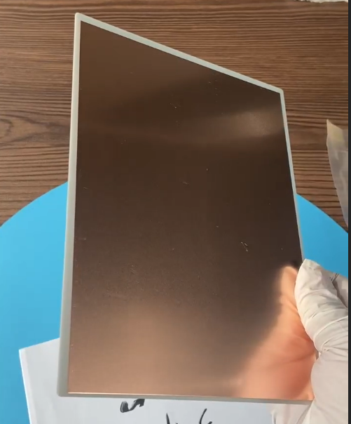
AMB ceramic copper-clad laminates are widely used as high-performance substrates in power electronics due to their excellent thermal conductivity, electrical insulation, and mechanical strength.
READ MOREHome>Industry>Semiconductor Industry
Vacuum brazing is essential in the semiconductor industry, where ultra-clean, high-precision bonding is required for the fabrication of advanced electronic components. It is widely used in the production of heat sinks, sensor housings, wafer processing tools, and vacuum chamber assemblies. The process enables the joining of dissimilar metals and complex structures without introducing flux or contaminants, making it ideal for maintaining the ultra-high vacuum and purity levels demanded in semiconductor environments. Vacuum brazing ensures superior thermal conductivity, structural integrity, and leak-tight sealing—critical for temperature-sensitive and high-performance semiconductor devices.


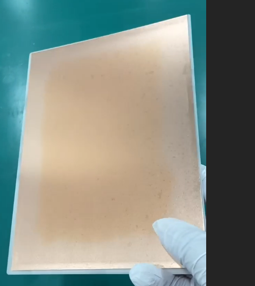
AMB ceramic copper-clad laminates are widely used as high-performance substrates in power electronics due to their excellent thermal conductivity, electrical insulation, and mechanical strength.
READ MORE
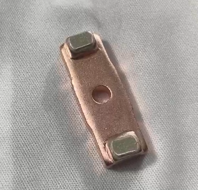
Copper provides excellent electrical and thermal conductivity at an economical cost, while silver enhances surface conductivity, contact reliability, and resistance to oxidation.
READ MORE
Vacuum brazing of AMB (Active Metal Brazing) ceramic copper clad laminate is a critical process used in the production of high-performance power electronic substrates.
READ MORE
AMB (Active Metal Brazed) ceramic copper-clad laminates are among the most reliable materials used in high-power electronics. Their unique combination of ceramic insulation and copper conductivity makes them ideal for applications such as IGBT modules, EV inverters, high-efficiency power supplies.
READ MORE